The Instruction for DCRC RevE Calibration and Tests
The Instruction is being moved to Confluence. Click here and check out.
This document was updated on Oct 22, 2019.
0 Preparation
0.0 Smoke Test
- Power the DCRC board and connect it to the Computer. Check the 5 LED lights are on.
Smoke Test. No Smoke: No critical Issues; Smoke: It's really bad. Report.
USB: initial setup, debugging, testing, firmware programming, etc
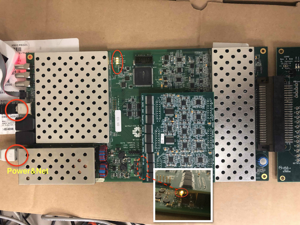
Power&Net: Power, data taking
0.1 Assign/Change an IP address via minicom
- Run the following commands in terminal:
$ minicom -D /dev/ttyUSB0 Ctrl+A +Z (release Ctrl and A before press Z)to show the Menu, then configure minicom(Select O)-->Serial port setup-->change the Hardware Flow Control to No(Select F). Enter to previous menu, then choose Exit.
Check the current IP.
Type
SETto check the current IP. (PS: TypeHEfor help. In the list popped out, SOCKET --> SET. )
Note: If screen shows nonsense when you type something, please change the baud rate: Press Ctrl+A +Z, then press P to get comm parameters menu. You will see the baud rate dispalyed at the top of the box: "Current: 9600 8N1" or something. "9600" is the baud rate. Press A to change the baud rate and then go back to try to type something. It will be the proper baud rate when the screen shows what you type.
Then assign a new IP addressand MAC address, if applicable.
SET 1 165.91.180.63to reset IP address for the DCRC;SET 2 165.91.180.1to reset the GateWay;SET 3 255.255.254.0to reset the NetMask;SET 4 a1.b2.c3.d4.e5.f6to reset the MAC address; (Notes:a1.b2.c3.d4.e5.f6is just the format. Copy the real MAC address that you see in Step 2, and then only change the last part. For board serial number 15, changef6to0f.0fis hexadecimal for 15.)NETSAVand thenSETto chekc if new IP address is saved.RESETthe board
Exit minicom with Ctrl+A then X
Disconnect the board
0.2 Load the firmware
Log in a firmware computer;
Download the script (Skip this step if you have downloaded it)
xxxxxxxxxx$ git clone ssh://yourusername@titus.stanford.edu:26/data/git/DCRC/load_firmware.gitand run this command.
xxxxxxxxxx$ ./load_firmware.py /dev/ttyUSB0 firmware_images/RevE.rbf --flashYou could download RevE.rbf from here, https://confluence.slac.stanford.edu/display/CDMS/DCRC+Documentation. Go to Rev E FPGA firmware, and click "Rev E FPGA firmware with L1 trigger".
(For the record, here is the old instruction for loading the firmware. )
1. Prequisite before DAC Calibration and Tests
1.0 Download the iphython git package.
Go the directory you'd like to download the git package. Here you need a SUF account. If this is your first time to talk to nero, you need to set up your account first by following STEP 2 in this link.
xxxxxxxxxx$ git clone --recursive ssh://nero.stanford.edu:26/data/git/DCRC/RevD_testbench.git$ cd RevD_testbench/$ git branch -av #Check which branch you are currently in$ git checkout --track origin/feature/jsw_DCRC_controls #CommentsCheck the Trigger_Simulation directory. If it is empty, run these two commands.
xxxxxxxxxx$ git submodule init$ git submodule updateTips: You could switch between branches you already have by the following commands as an example. It's unnecessary for this procedure of Calibration and Tests.
xxxxxxxxxx$ git branch -av #Check which branch you are currently in$ git checkout master #Switch to another branch 'master'$ git branch -av$ git checkout feature/jsw_DCRC_controls #Switch to branch 'jsw_DCRC_controls'If you change the code and want to push the change to git repository, check here for the procudure.
1.1 Necessary Materials for Calibration and Tests:
DCRC Test Bench (python notebook) (Done in "1.0 Prequisite before DAC Calibration and Tests")
Oscilloscope and Function generator. (Both included in picoscope.)
Multimeter
- DCRCRevD.1 probe points (just for record)
- DCRCRevE probe points (same link as 1. DCRC Checklist and Calibrations Spreadsheet)
Issues&Solutions (You may find the solution when you have an issue)
2. Calibration
2.1 Purposes
Check the slopes and find the offsets, and their uncertainties. Fill the values into "DCRC Checklist and Calibrations Spreadsheet" and make a MIDAS file.
Slopes:
- Driver Offset, LockPoint, SqdBias, QOffset: 0.125 mV/step
- DDSMagnitude: 1.85mV/step
- QETBias: 0.0825 mV/step (measured at miniBob with the 100k resistor)
- QBias: 0.42725 mV/step (measured at miniBob)
- LEDMagnitude: 2.44 mu A/step (though this one is not as strict because it's a bit different, but also, nobody really will calibrate on LED luminosity...)
2.2 Procedure
2.2.0 Preparation
- Setup the python notebook
- Make sure that all 5 LEDs are turned on. If not do RESET by
$ minicom(See 0.1 Assign/Change an IP address via minicom) - Open the relavant code file and Run the code cell by cell. Note: There are three code files, Test_Signal.ipynb, DCRC Calibration.ipynb and LED.ipynb, with the order consistent with the contents in the spreadsheet.
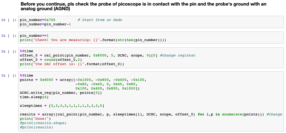
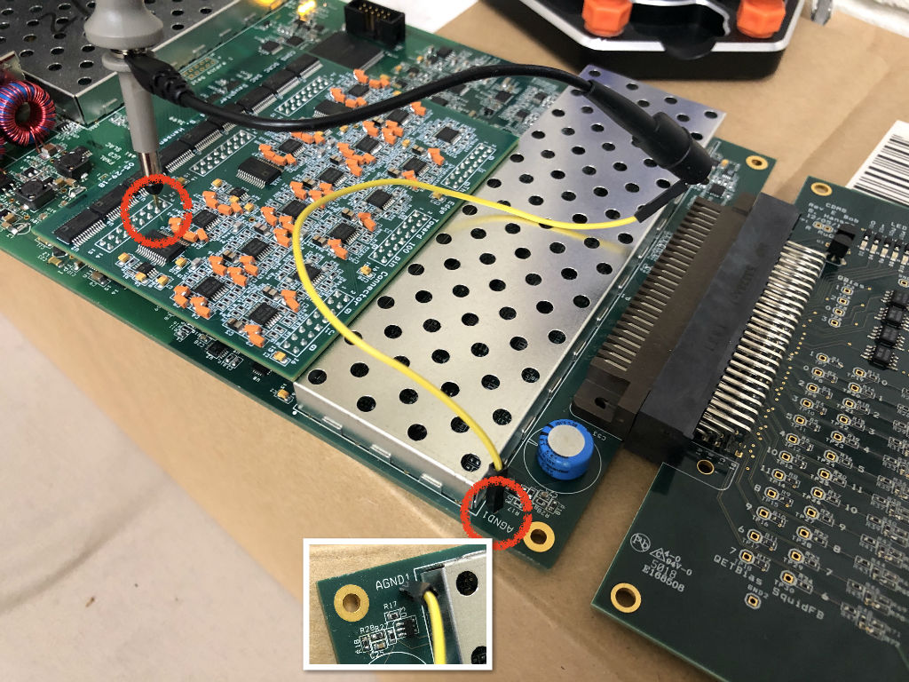
- When you see the below code cell and you are ready to run, make sure keep the probe of picoscope in contact with the pin you are going to measure, and connect the probe's ground to an analog ground (AGND), like the picture below showed. (There are several AGNDs. Using any one is OK.)
2.2.1 Test Signal Calibration
Open Test_Signal.ipynb and run the code cell by cell.
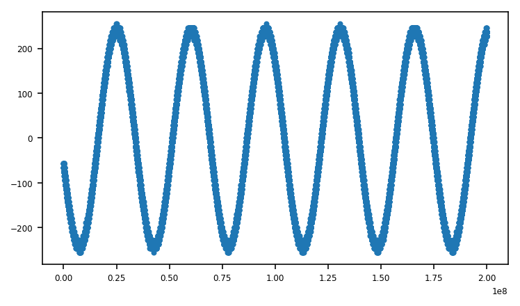
Under the first cell in ADC Calibration, you should see a plot of sine wave as below. If not, please check if there is something you did incorrectly.
if you see the sine wave, keep running the code. when you are done, open LEC.txt and the results will be at the last line in it. You will see a line like "3 0.238497 0.000104 20.373681 0.217045". They are "LED# slope slope_uncertainty offset offset_uncertainty", respectively.
2.2.2 the most Calibration
- Open DCRC Calibration.ipynb and run the code cell by cell.
- You will find the results under this code cell. As you see, they will be written in a txt file (here using SN19 as an example) automatically, which will make it easier for you to copy and paste into the calibration spreadsheet.
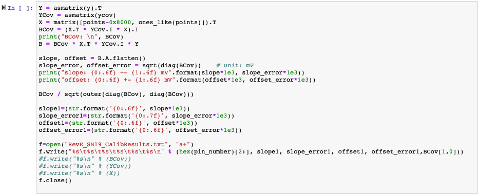
- At the end of the code you will see the plot of Measured Values vs Expected Values. Visual Check: ALL the datapoints should follow the fitting line.

- Repeat the above steps for the other pins. Don't forget to change the expected_slope here before measuring the pins of another category. (Categories: DrvOffset, LckPnt, SqdBias, QETBias, QOffset, QBiasDac.)
- In the current version of code, you needn't change register/pin number (i.e.
0x760) when measuring the pins in the same category. If you need to redo the measurement, change the register/pin number in the first cell in the picture in 2.2.0 Preparation. - Make sure you have killed the python notebook after finishing tests. The scope will not work next time if you do not kill python notebook before leaving. If you can't talk to picoscope, make sure nobody is using it and disconnect the USB port of the scope from the computer. Wait for few seconds then connect it again.
2.2.3 LED Calibration
- Open LED.ipynb and run the code cell by cell.
- Under the first cell in ADC Calibration, you should see a plot of sine wave as below. If not, please check if there is something you did incorrectly. It's highly possible the connection is bad.
You will find the results somewhere, see the 1st picture in 2.2.2 the most Calibration, or at the last line of LED.txt
2.3 Midas Calibration File
Making the midas calibration file is the final step when you have all of the calibration values. You need to create a text file with the HEX-values for the calibrations, space-separated, all in a single line. The format telling you the order of the registers is shown in the calibrations google-doc spreadsheet, under the MIDAScal sheet. Then, MIDASworksheet page does the formatting from our DACCalibs sheet. (All these are the sheets in the spreadsheet document, see example below)
Then you need to push the calibration file into the gitblit MidasDAQ repository, under the path: / online / src / DCRC / calibrations The file should be named: revXX_YY.cal ;
XX = DCRC version (D, D1, E, etc)
YY = DCRC serial number (14, 15, 1, etc)Take a look at the RevD.1 calibrations for an example: - calibration file: revD1_14.cal
- Spreadsheet, see sheet: MIDAScal
You can see the Midas ranges and corresponding physics values in Midasworksheet. For example, for ADCoffset Midas range is 0x0000-0xFFFF (hex) and voltage range is (-4v)-(+4v). You can get the Default Slope by dividing the range in mV to the range in hex. In this case, 8000 mV/HEX2DEC("ffff")=1.221E-01mV/step. You can see that we multiply the slope by the factors in column k. This is only to make sure that we can get a 4 digit hex number to put in the midas file and we should keep track of this. We want the offset from 8000 because it is the middle of the limit, so ideally, the offset should be a value around 8000 hex.
3. Tests (Noise, Phonon, Charge and Trigger)
(Trigger test is included in Phonon Test and Charge Test)
- Run these python files, DCRC Noise Performance.ipynb, DCRC Phonon Signal Test.ipynb and DCRC Charge Signal test.ipynb, to test the noise, phonon and charge seperately.
- Check if the plots show the expected results
3.1 Noise Performance
Test the noise performance for ALL channels. Channel 0~11 are phonon channels and Channel 12~15 are charge channels. When you run the code, it will show the traces and PSDs of all channels. Check them visually.
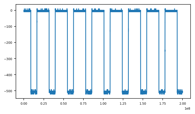
- Check the Trace visually. There should be just random noise and no signals of some specific pattern. The first one is an example of the noise trace for a phonon channel; the second one is for an charge channel; the third one includes the traces of all channels.


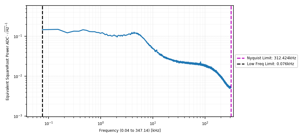
- Check the PSD. (upper: a phonon channel; lower: a charge channel. Input Gain: -0)

3.2 Phonon Tests
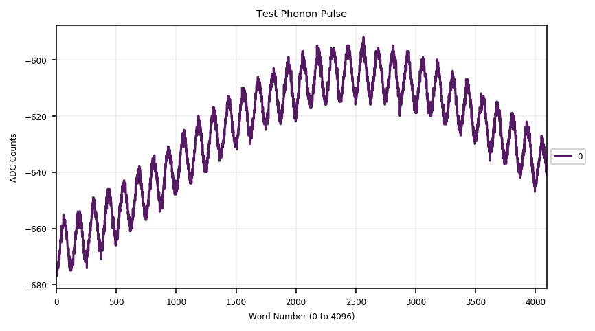
Test Input Gain on test signals. Visually check: the baselines and the amplitudes are supposed to be ×1, ×2, ×4 with Input Gain 16, 32, 64. Here is the plot with Input Gain 16.

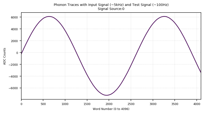
Check both the Test Signal (by the signal generator inside DCRC, low frequency) and the Input Signal (by picoscope, high frequency) work.
Check the source switch and output. Source 0: Feedback; Source 1: PreAmp. Here are the two example plots. The upper is with Source 0 and the lower is the Source 1.

Feedback Gain is removed in RevE.
Check the Drive Gain for every phonon channel. Visually check: the baselines and the amplitudes are supposed to be ×1, ×2, ×4, ×8 with Driver Gain 0, 1, 2, 3. Here is the example plot of Channel 0 with Driver Gain 0.

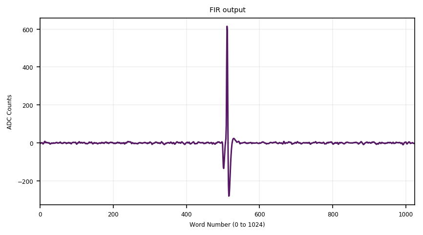
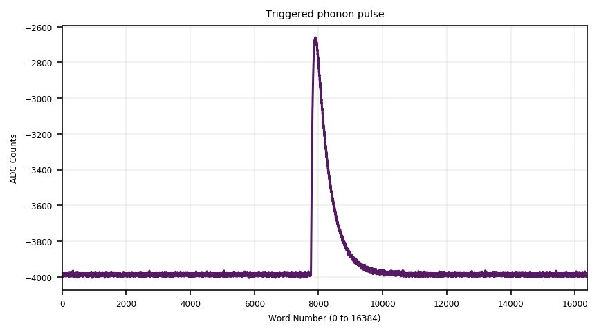
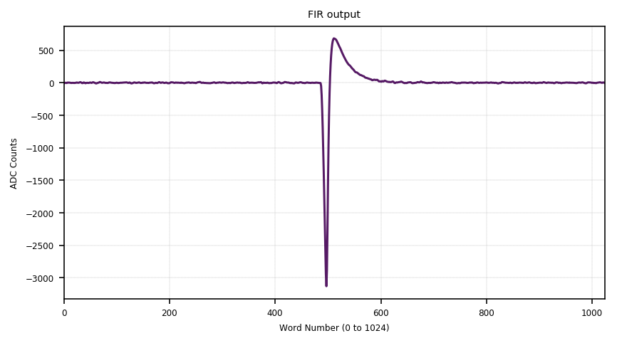
Trigger Test: Check the triggered pulse and FIR output


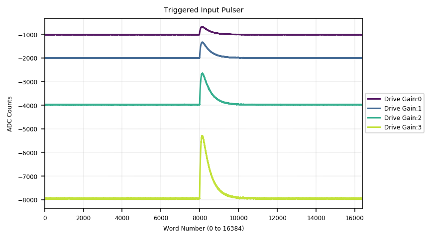
Trigger Test: Check Driver Gains on the input pulse. Visually check: the baselines and the amplitudes are supposed to be ×1, ×2, ×4, ×8 with Driver Gain 0, 1, 2, 3.
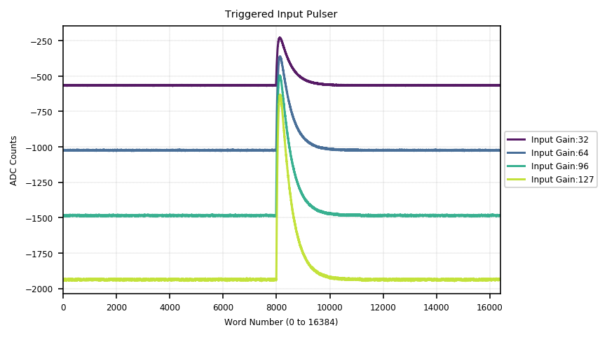
Trigger Test: Check the Input Gain on the input pulse. Visually check: the baselines and the amplitudes are supposed to be ×1, ×2, ×3, ×4 with Input Gain 32, 64, 96, 127.
ALL the results above are from the test on Phonon Channel 0. The next is to do the same on ALL phonon channels one by one. Note: You are going to do twice, one with Source 0 (Feedback) and one with Source 1 (PreAmp), as you will when doing the test. Visually check using the standard above.
Test Signal Trigger. Visually Check: you will the plot like below.

3.3 Charge Test
Change the offsets and see its effects.
Here is the plot showing the offset change works. The end value of one trace should be the starting value of the next trace. Check it visually. (Order: blue, yellow, green, red)

Trigger test with the charge pulser
You will see plots like the following if the DCRC passes the trigger test with the chrage pulser. Check for ALL four charge channels.


Trigger test with the input pulse
You will see plots like the following if the DCRC passes the trigger test with the input pulse. Check for ALL four charge channels.